Before going further, let’s put here a list of related posts. Although not required, I encourage you to go through them all before reading the following post.
- Scale-Out And Scale-Up Architectures – The Business-Critical Application Point Of View
- Two Main Scale-Up Server Architectures – Part 1
- Two Main Scale-Up Server Architectures – Part 2
- Bull’s Implementation of a Glued Architecture
OK now let’s deep dive this BCS technology. I ended up my previous post by saying that Bull’s BCS solves scale-up issues without compromising performance. Here a graph showing what that does mean.

Bullion measured performance vs the maximum theoretical performance – Specint_rate 2006 – Courtesy of Bull
Bull’s BCS eXternal Node-Controller technology scales up almost linearly compared to the ‘glueless’ architecture. What’s the secret sauce behind this awesome technology?
BCS Architecture
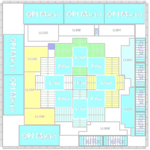
The BCS enables two key functionalities: CPU caching and the resilient eXternal Node-Controller fabric. These features server to reduce communication and coordination overhead and provide availability features consistent with Intel Xeon E7-4800 series processor.
BCS meets the most demanding requirements of today’s business-critical and mission-critical applications.
As shown in the above figure, a BCS chip sits on a SIB board that is plugged in the main board. When running in a single node mode, a DSIB (Dummy SIB) board is required.
As shown in the above figure, BCS Architecture scales to 16 processors supporting up to 160 processor cores and up to 320 logical processors (Intel HT). Memory wise, BCS Architecture supports up to 256x DDR3 DIMM slots for a maximum of 4TB of memory using 16GB DIMMs. IO wise, there are up to 24 IO slots available.
BCS key technical characteristics:
- ASIC chip of 18x18mm with 9 metal layers
- 90nm technology
- 321 millions transistors
- 1837 (~43×43) ball connectors
- 6 QPI (~fibers) and 3×2 XQPI links
- High speed serial interfaces up to 8GT/s
- power-concsious design with selective power-down capabilities
- Aggregated data transfer rate of 230GB/s that is 9 ports x 25.6 GB/s
- Up to 300Gb/s bandwidth
Each BCS module groups the processor sockets into a single “QPI island” of four directly connected CPU sockets. This direct connection provides the lowest latencies. Each node controller stores information about all data located in the processors caches. This key functionality is called “CPU caching“. This is just awesome!
More on this key functionality in the second part. Stay tuned!
Source: Bull, Spec.org


Pingback: Bull’s BCS Architecture – Deep Dive – Part 2 « DeinosCloud
Pingback: Bull’s BCS Architecture – Deep Dive – Part 3 « DeinosCloud
Pingback: Bull’s BCS Architecture – Deep Dive – Part 4 « DeinosCloud
Pingback: VMworld 2013 | vmdude
Pingback: VMworld 2013 | vmdude
Pingback: Physical Network Connectivity Lost And Intel® 82599 10 Gigabit Ethernet Controller | DeinosCloud